




From island to island: this is how energy travels through a fragmented crystal
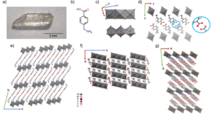
- A research team from IMDEA Nanociencia, in collaboration with UAM, and centers in the Basque Country and Catalonia, has described a two-dimensional perovskite whose inorganic layer is not continuous but rather an archipelago of islands.
- Despite this, the absorbed light energy travels through the material at a speed comparable to that of conventional perovskites, jumping from island to island.
| Tweet |  |
Press release download |
Madrid, 23 rd september, 2026.
A team of researchers from the Autonomous University of Madrid (UAM), IMDEA Nanociencia, and several centers in the Basque Country and Catalonia has synthesized a new material from the perovskite family—materials used in the next generation of solar panels, LEDs, and light detectors. What makes it unique is that the energy it absorbs from light is transferred very efficiently, even though its internal structure is “broken up” into small islands.
The study, led by Raquel Utrera Melero and Ferry Prins of the Center for Condensed Matter Physics (IFIMAC) and the Department of Condensed Matter Physics at the UAM, along with Jose Sánchez Costa (IMDEA Nanociencia) and Beatriz Martín-García (Ikerbasque and CIC nanoGUNE), is published in the journal *Advanced Materials*.
Archipelago Instead of a Sheet
Two-dimensional perovskites resemble puff pastry: extremely thin layers of lead and bromine alternate with layers of organic molecules. Normally, the lead-bromine layer is continuous and functions like a highway along which energy flows freely
.
In the new material, the organic molecules—4-aminomethylbenzoic acid—are held together by very strong hydrogen bonds. This bonding makes the structure so rigid that the inorganic layer fails to form completely: it fragments into identical islands consisting of just three pieces, aligned like dominoes and separated from one another by the organic molecules. The researchers confirmed this orientation by illuminating the crystal using polarized light and analyzing how their atoms vibrate, a technique known as Raman spectroscopy.
Jumping from Island to Island
With a structure like this, one would expect the energy to be trapped on each island. To test this, the team shone a laser on a tiny spot on a crystal wafer and observed, using a microscope capable of recording changes in billionths of a second, how the light spot spread out over time.
“The result surprised us, because the excitons—the ‘packets’ of energy created when light is absorbed—travel about 180 nanometers in one direction of the crystal and about 90 nanometers in the perpendicular direction,” explains Raquel Utrera, a researcher at the UAM. “In the fast direction, they diffuse three times faster than in the slow direction, and at a rate comparable to that of well-known continuous perovskites.”
The key lies in how they move. In conventional perovskites, energy travels in a delocalized manner through the continuous layer. Here, however, each island acts as a tiny antenna that passes energy to its neighbor without actually touching it, much like one tuning fork can cause another nearby one to vibrate. This mechanism is known as resonant near-field energy transfer. According to the measurements, each exciton makes on the order of ten trillion jumps per second.
The electromagnetic simulations conducted by Antonio I. Fernández-Domínguez of the Department of Theoretical Physics of Condensed Matter at the UAM support this explanation. Furthermore, they reveal an interesting detail: in the direction where the islands are closest to each other, the jumps are more frequent, but in the opposite direction, each jump covers more than twice the distance, which is why energy travels faster in that direction.
A New Approach to Designing Materials
The study demonstrates that a continuous lattice is not essential for efficient, directed energy transport in these materials. This opens the door to designing energy transport independently of how the atoms are connected, which could be harnessed to channel energy in optoelectronic devices. The remaining challenge is stability: the material degrades rapidly when exposed to ambient humidity, and the team is already working to improve it.
Reference:
R. Utrera-Melero, A. Cutrupi, I. Rivilla, D. Spirito, E. C. Sañudo, J. Cabanillas-González, A. I. Fernández-Domínguez, B. Martín-García, J. Sánchez Costa, F. Prins. Efficient In-Plane Exciton Transport in a Discontinuous Layered Lead-Bromide Perovskite. Advanced Materials e75282 (2026). DOI: 10.1002/adma.75282
 https://hdl.handle.net/20.500.12614/4289
Contact:
José Sánchez Costa
Switchable Nanomaterials
This email address is being protected from spambots. You need JavaScript enabled to view it.
IMDEA Nanociencia Dissemination and Communication Office
This email address is being protected from spambots. You need JavaScript enabled to view it.
+34 91 299 87 12


Source: IMDEA Nanociencia.
IMDEA Nanociencia Institute is a young interdisciplinary research Centre in Madrid (Spain) dedicated to the exploration of nanoscience and the development of applications of nanotechnology in connection with innovative industries.